1-to-2 lvcmos / lvttl fanout buffer w/ complementary output.
* Complementary LVCMOS / LVTTL output
* LVCMOS / LVTTL clock input accepts LVCMOS or LVTTL input levels
* Maximum output frequency: 250MHz
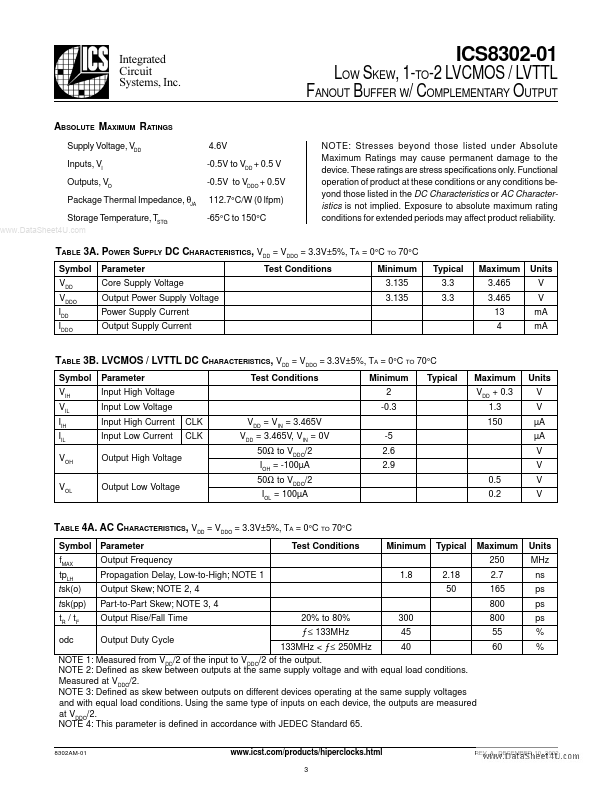
* Output skew: .
demanding well defined performance and repeatability.
,&6
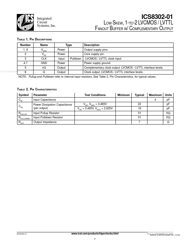
BLOCK DIAGRAM
Q CLK nQ
PIN ASSIGNMENT
VDDO VDD CLK GND 1 2 .
T h e I C S 8 3 0 2-01 i s a l o w s k e w, 1 - t o - 2 LVCMOS/LVTTL Fanout Buffer w/ComplemenHiPerClockS™ tary Output and a member of the HiPerClockS™ family of High Performance Clock Solutions from ICS. The ICS8302-01 has a single ended clock input.
Image gallery
TAGS
Manufacturer
Related datasheet
 Download (Size : 110.83KB)